There are a few steps to use the digital IO of the MSP430.
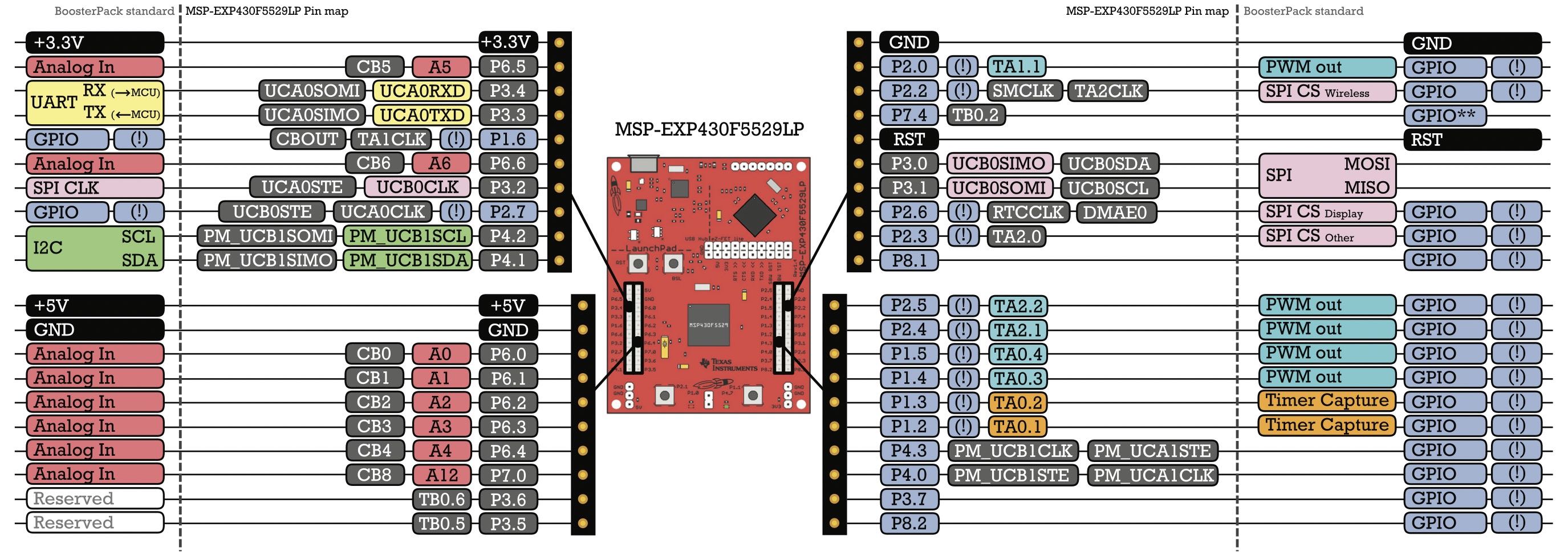
The pinout of the MSP-EXP430F5529LP launchpad can be found in the official TI website :

In addition, the LEDs and push buttons are connected to:
| Component | Port |
|---|---|
| Red LED | P1.0 |
| Green LED | P4.7 |
| B1 (left) | P2.1 |
| B2 (right) | P1.1 |
Digital inputs/outputs
The launchpad (or the microcontroller) can be connected to various electronic components, such as buttons, LEDs, integrated circuits, ...
The digital I/O can have 2 states :
- high (or 1, or ON, or true)
- down (or 0, or OFF, or false)
Ports
The MSP430F5529 has 6 8 bytes-ports, or 3 16 bits-ports:
- Port 1 to 6 : 8 bits ports
- Port A (includes ports 1 and 2), Port B (includes ports 3 and 4), Port C (includes ports 5 and 6)
Each pin is identified by the byte corresponding to its position : P3.1 is the bit 1 of the port 3.
To help the developers to write code, those definitions are present in msp430.h (in C or asm):
#define BIT0 0x0001 // 0000 0001 in binary
#define BIT1 0x0002 // 0000 0010 in binary
#define BIT2 0x0004 // 0000 0100 in binary
#define BIT3 0x0008 // 0000 1000 in binary
#define BIT4 0x0010 // 0001 0000 in binary
#define BIT5 0x0020 // 0010 0000 in binary
#define BIT6 0x0040 // 0100 0000 in binary
#define BIT7 0x0080 // 1000 0000 in binary
If the MSP430 you are using contains a FRAM, its content doesn't vanish after powering off or resetting it. So, do not assume that all the register will contain 0x00. It's important to set all the values avoiding using values coming from the last execution.
The direction registry (PxDIR)
This register defines if the pin we are configuring will be an input or an output. There is a register per port : P1DIR, P2DIR, ...
Setting a bit to 0 will configure the pin as an input. Setting it to 1 will configure the pin as an output.
For example, to configure the port P1.1 as an input, P1.0 and P1.2 as output, ce can proceed : in asm:
    bic.b    #BIT1, &P1DIR     ; set the P1OUT's 1st bit to 0
    bis.b    #BIT0, &P1DIR
    bis.b    #BIT2, &P1DIR     ; set the P1OUT's bit 0 and 2 to 1

    ; bic clears the bit and bis set the bit
    ; PxDIR are 8 bits registers, so we will work with bits by using operand.b
    ; #BIT1 is the immediate value of bit1
    ; P1DIR stores the address of the register in the memory.
    ;      To change the bits of the register, we use the "&" operator
in C:
    P1DIR &= ~BIT1;    // Simpler... Just bitwise operations!
    P1DIR |= BIT0 + BIT2;
The Output register (PxOUT)
Nothing simpler than setting the bit corresponding to the pin to 1 or 0 to set the output in the high or low state! Each bit of the register corresponds to a logic level of the port's bit.
The Resistor Enable register (PxREN)
If a pin is set as an input, it's important to set up a pull up or a pull down resistor.
The MSP microcontroller includes such resistors, avoiding us to include it in our schematics. There are ~35kΩ resistor (in fact it can be a value between 20 and 50kΩ) that can be used as a pull up or pull down resistor.
Pull up resistor
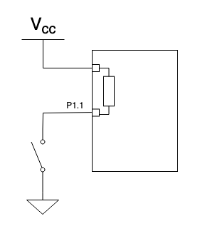
It's the more common one:
- It is connected between the VCC and the input pin
- by default, the input is in a high state
- it's usual to place a button between the input pin and the groud : when pressed, the level is low:

Pull down resistor
- connected between the input pin and the ground
- keeps a low input level
- If we connect a button between Vcc and the input pin, when pressed, the input level is high
Configuration of the pull up / pull down resistor
To activate the resistor, the PxREN bit corresponding to the pin has to be set to 1.
The PxOUT register is used to chose if we set a pull up or a pull down register (the pin is configured as an input, so we won't change the logical level of the pin when changing PxOUT). When PxOUT is set to 1, we configure a pull up restistor. When set to 0, we chose a pull down resistor
Configuring P2.1 as an input with a pull up resistance can be done with this code:
Using assembly:
    bic.b   #BIT1, &P2DIR       ; Set P2.1 as an output
    bis.b   #BIT1, &P2REN       ; enable the pullup/down resistor
    bis.b   #BIT1, &P2OUT       ; set the resistor as a pullup
Using C:
    P2DIR &= ~BIT1;
    P2REN |= BIT1;
    P2OUT |= BIT1;
The input register (PxIN)
This register is a read only register. Each bit of PxIN corresponds to the logic level of the pins of the port
Wrapping it up
| PxDIR | PxREN | PxOUT | Configuration |
|---|---|---|---|
| 0 | 0 | x | Input. The electrical circuit will have to include the needed components to avoir having an unknown input level |
| 0 | 1 | 0 | Input with pulldown resistor |
| 0 | 1 | 1 | Input with pullup resistor |
| 1 | x | x | Output |
Comments !